For a while I had been looking into the Kenbak-1 computer, admiring how much can be achieved with such basic logic circuits compared to the alternatives in 1971. Having been taught the importance of shift registers at University I was pleased to see them in use throughout the Kenback-1 architecture
While chatting to a friend in Canada one evening I mentioned I would like to learn how to program an MCU and make a processor actually do what I want for once. Being an electronics engineer, I work with basic logic chips all the time, but as I repair electronics and only design basic logical test gear, I had never got round to looking at the possibilities of a PIC chip, MCU’s or CPU-VIA designs. Explaining this to a friend from Canada one evening, he suggested I obtain an Arduino-Uno development PCB and start playing. 2 weeks later and I had managed to write two programs; one to flash and LED on and off, the other to control a steam boiler with a variable jet and display what it is doing on a graphic display with bar charts etc.
I happened to mention this fantastic new device I had discovered to Mike in general catch-up email and I was surprised by his quick reply, stating how someone called Mark Wilson had designed, built and programmed a Kenbak-1 Emulator based on the ATMega328 MCU. This just happens to be the MCU the Arduino-Uno uses. Mike enquired if I could make one, how much, and when can I build it.
After reading Mark’s very intuitive write up of his Kenbak-1 emulator, I priced up the work (parts only), agreed with Mike and set to work drawing the circuit diagram into my PCB program. I have to take my hat off to Mark, his skill of being able to draw circuit diagrams in ASCII is amazing. My ability to read them properly needs much improvement! While designing the PCB layout based on my modifications (such as a power supply and USB interface), I was able to e-mail Mark who was very helpful and also suggested I email John Blankenbaker, the designer of the original Kenback-1. John was enthusiastic for the project, and also asked if I could make sure I made a couple of improvements he always meant to do.
With the PCB designed the parts on order, I then had the most difficult job of all; make the printer print on acetate sheet! At £1 a sheet it is not good to make many mistakes! Two hours later I finally had a printer which would not only feed the acetate sellotaped to paper through, but also print on it as well. With the printer dealt with I could get on with making the PCB, at least this bit is easy! 5 minutes per side in the UV box, through the photo developer and into the Ferric Chloride. 3 hours later, just got to drill 100 holes with a 0.8mm drill bit.
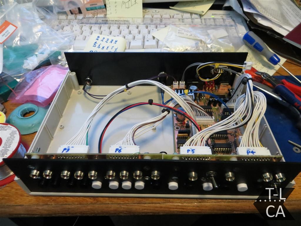
After drilling the 100+ holes, correcting the minor errors such as top side track touching the heatsink, and topside track under a capacitor where you can’t solder, it only took 1 hour to solder the components to the PCB. Onto the same process with the front panel PCB for the buttons, only this time it was made in two halves from the same PCB, cut out and soldered together. A short time later and both PCB’s were made. Most people would probably stop at this point, being 3am, but I just continue until the job is done. By 6am I had made the wiring looms (they take a long time!) and decided I should think about going to bed, otherwise I may be accused of staying up all night.
Most people don’t realise the mind never sleeps. I suspect people drink alcohol to quieten it down, but being tea-total I don’t have that luxury. By 10am I woke up with a picture in my mind: That PCB is going to hit the buttons. D’oh! As usual my inner subconscious has made me look a fool. I decided to plug everything in anyway, you never know it may be an easy fix. There was a slim possibility of it fitting, so onwards to the power switch for its glorious first power up. Of course nothing happened.

Being a PCB repair engineer I am quite used to this. 1st rule for repairs, check the power. Nothing. 12V into the regulator, nothing out. It is at this point I realised I had the regulator component rotated 180 round the wrong way, and had put 12 volts into the On/Off input. It did not like this very much and decided to stop working. No magic white smoke came out so I can only assume it just lost its spin inside the chip. New regulator, the right way round this time, and the Kenbak-1 emulator lit up like Blackpool illuminations.
My first observation was the push-button switches appear to be shifted 1 position to one side, with the last button now being the first. Or in other words, I had mis-read the datasheet compared to Marks ASCII drawing. Mark’s D0 was called Q1 on the Datasheet going to Pin 2 on the IC. My dyslexic brain just couldn’t handle it! Not to worry though, an easy fix by moving the wires in the wiring loom. 5 minutes later and the LED’s now matched the switches, or are they?! Someone must have re-arranged my circuit diagram while I wasn’t looking, because somehow the LED’s for the switch indicators were all over the place. It is at this point I realised the component on my PC had all its pins miss-named. Something I had spotted for the Bit LED’s but had then forgotten about for the command LED’s. It was at this point I remembered that I had remembered to write myself a note to remind me to remember to change the component pinout. Not to worry though, 5 minutes on the wiring loom had it sorted.
Now I have all the buttons working and all the LED’s flashing, and when I press the Bit 0 button, Bit 7 LED lights up.
Who soldered that connector on backwards?
By this time I have had enough. I took the PCB out, as it was never going to fit properly with the front panel PCB, remembered to remember to change the 165 component on the PC and re-designed the PCB, with the corrected circuit diagram. This time I sorted all the previous issues, printed the PCB onto the acetate sheet 1st time and etched a new PCB. While waiting for the PCB to etch I re-wired all the wiring looms back to normal and took all the components off the original PCB (I left the few resistors and all the chip holders). Also with a quick re-arrangement of the furniture I was able to hide the Ferric Chloride stain on the carpet. She’ll never know. By 6pm I had a brand new PCB, all working and fixed to the enclosure. It is satisfying when something like that goes right.
The front panel was only half complete at this point. I had designed into it a system of enabling and disabling the Lock/Unlock option for each button. After spending half an hour soldering the jumper posts to the WRONG side of the PCB, I then spent an hour taking them back off and soldering them to the correct side. Finally with everything complete I was able to give the Kenbak-1 Emulator a proper run. Only now none of the buttons work.
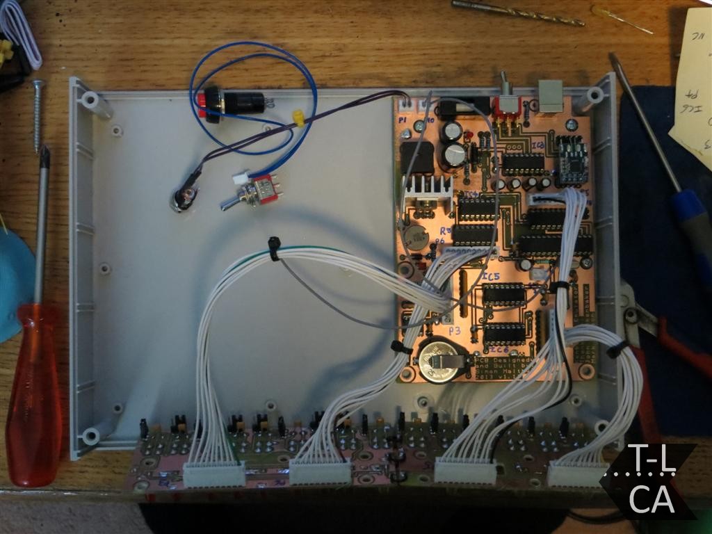
A quick check reviled that in fact all the buttons were on. It is here where I realise I had connected one line on the circuit diagram to node 351 instead of 352. This wouldn’t usually be a problem, except 351 was the earth plane, which spanned most of the Front Panel PCB. This means that 99% of the unused space on the PCB was now firmly attached to the jumper posts I had just spent half an hour soldering on the wrong way round, followed by an hour to sort them out. I worked out the minimum amount of track I would have to cut to separate the top earth plane from the bottom. Fortunately it wasn’t too bad and I had the two separated and re-routed, both sides, within an hour.
Finally, the PCB and Front Panel PCB were not only complete, but correct. All tests showed the inputs were going in, the outputs were going out, and even the USB UART module was working after some micro-soldering repair.
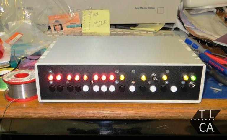
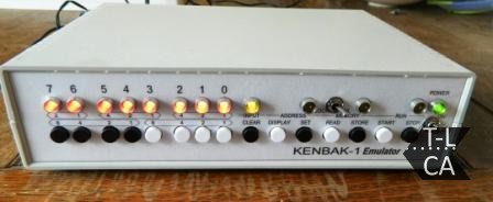
A quick swing by my workshop saw the plastic panel for the front of the enclosure drilled out ready for the switches, LED’s and mounting screws. It took a while to persuade all the screws to hold themselves in place while I attached the front panel PCB, but it made a for a very sturdy switch panel. Using CAD to print out the switch positions taken directly from the PCB program ensured the holes lined up with the switches, LED’s and fixing screws. Then a nicer-looking print out was laminated and cut to size for the front panel legend. The front panel was then persuaded into the enclosure bottom, the nicely laminated legend making it a little tight. Then with the rear panel cut out and in place, the lid was fitted and the Kenbak-1 Emulator was finished, largely thanks to John Backenbaker and Mark Wilson.